How to Ensure Proper Grounding in Rigid Flex PCBs
Proper Grounding in Rigid Flex PCBs
Rigid flex is a PCB that’s often used in mobile devices and other products with small footprints. It’s a hybrid type of PCB that combines elements of rigid circuit boards with flexible circuit boards to produce a board that can be bent or folded. This type of PCB offers a lot of benefits over traditional rigid circuit boards, and it can help make your product more compact and versatile.
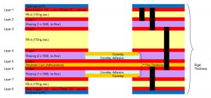
One of the most important aspects to consider when designing a rigid flex is proper grounding. It’s crucial to make sure your traces are properly grounded to avoid issues like signal interference and short circuits. This can be accomplished by using a plated-through hole (PTH) with a 10 mil annular ring around it, or by placing a grounding pad on the surface of the board.
Another critical factor to consider when designing a rigid-flex is the layout of its copper layers. It’s important to use a dense copper plating to ensure that your traces have enough strength and conductivity, which will prevent them from being impacted by mechanical stresses during the bending process. Using a dense copper plating also helps to reduce the risk of oxidation and other problems that can impact a PCB’s performance.
How to Ensure Proper Grounding in Rigid Flex PCBs
The most common cause of failure in a flex circuit is the formation of a crack within the copper. This can be caused by a number of factors, including stacked traces and excessive bending. Stacked traces happen when two or more traces are placed on top of each other, and they can expose the outermost trace to undue stress that can crack it. The best way to avoid this is to not stack traces in the flex and bendable sections of your circuit, and to follow proper bending guidelines.
A third problem that can occur with a flex circuit is the lifting of its copper traces. This happens when the traces are exposed to mechanical stress, and it can cause the conductive layer to fail. To prevent this, it’s important to design your traces with sufficient thickness and length, as well as to use a low/no-flow prepreg in the flex section of the PCB.
It’s also a good idea to use a hatched copper pour to reduce the amount of stress on your traces during bending. This will reduce the chance of flex fracture and increase their lifespan. Moreover, it’s also a good idea to use the right layer stacking for your flex circuit, and to add a protective shielding film for added durability and reliability.
Working with a rigid-flex PCB can be challenging, but it doesn’t have to be. With the right MCAD and ECAD tools, it’s easy to create a rigid-flex circuit that will work seamlessly with your device’s enclosure. With a 3D view of your bending region, it’s also much easier to prepare your flex circuit for manufacturing and generate Gerber files. Altium Designer is the only design software that combines these features into a single application, making it easier than ever to take your rigid-flex PCB from concept to production.